RSS

Tag Archives: lithography

Different resolution enhancement techniques for lithography


In the trends of miniaturization, resolution has become the main critical aspect for lithography process. There are some interesting techniques which help in resolution enhancements and if we combine some of these techniques, we have still possibility to go below 22 nm technology node.

1. Off-axis illumination : In off-axis illumination, the light passes through mask at an oblique angle rather than perpendicularly i.e. light,in this case, is not parallel to the axis of the optical system. This causes all the diffraction orders of light to be tilted and more higher orders are able to pass through the projection lens. As, we know higher order of diffraction contains fine details of images that’s why by this technique, we can get better quality images on the substrate.

2. Optical proximity correction: This is also photo lithography enhancement technique which is used to compensate the errors in the images due to diffraction or process effects. Lens normally acts as low pass filter in which limited amount of higher order spatial frequencies passes for image formation. So, imaging close to the resolution limit of the optical system, we face different errors in the images due to loss of finer details of image which can be provided by higher order spatial frequencies. Errors are actually due to inability of lens to maintain edge placement integrity of the original design causing rounding at the corners, shortening of line at the end, line width roughness, etc. In dense line, lens capture only zero and first order diffraction (not higher order diffraction) so that it causes imbalance in image formation. From optical proximity enhancement techniques, we can solve this problem. If the line on the wafer is thin, we make it thicker on the mask, if lines are too dense on the wafer, we do reverse on the mask, if line is too short, we make it long on the mask. For maintaining edge at the corners, we can place serifs ot hats at the corners on mask.

3. Phase shifted mask: Phase shifted mask are designed to sharpen the intensity profile or thin resist profile, which allows to sharpen the image to be printed. In alternating phase shifted mask, each alternate windows are 180 degree phase shifted in comparison to theirs neighbors so that the effect of adjacent light diffraction will have minimum effect to get sharpen image.

4. Immersion Lithography: In this case, immersion fluid passes between wafer and lens continuously so that lens substantially changes the light path, which enables higher angles of the incident light i.e image can have more finer details. This causes numerical aperture of lens to be larger than 1 thereby improving the resolution.
 
Leave a comment

Posted by on July 1, 2011 in CMOS fabrication


Tags: , , , , , ,

Extreme Ultraviolet Lithography


– MY B.TECH. SEMINAR (ABSTRACTS)

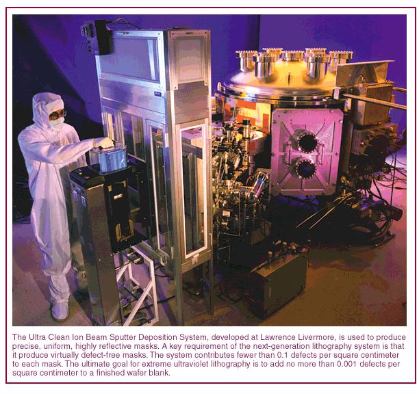
This paper mainly focuses on  the fundamental concepts and existing state of development of Extreme Ultra-Violet lithography (EUVL), an alternate optical approach, for sub-100-nm generations lithography process that uses extreme ultraviolet (EUV) radiation with a wavelength in the range of 10 to 14 nanometers (nm) to carry out projection imaging. Currently, and for the last several decades, optical projection lithography has been the lithographic technique from which the high-volume of integrated circuits has been manufactured. It was widely anticipated that improvements in this technology will allow it to remain the semiconductor industry’s workhouse through the 100 nm generation of devices. Extensions of optical lithography have been made possible by a continuous reduction in the operating wavelength and simultaneous increase in numerical aperture (NA). However, when the operating wavelength is reduced below 150 nm, all materials become opaque, requiring the use of reflective designs with optics using special coatings to achieve high reflectivities at the operating wavelength.  Also, National Technology Roadmap for Semiconductors (NTRS) has presented four new approaches for sub-100 nm generations lithography, called the “New Generations Lithographies” and they have demonstrated feasibility and are in various stages of subsequent research and development. EUVL is  one such technology vying to become the successor to optical lithography.

To a large degree, EUVL has been made possible by the development of advanced Mo-Si multi-layer coatings due to which optimum reflectivities are achieved. Moreover, by modifying the camera design, EUVL could meet the lithographic challenge of defining the minimum geometry Si-transistor deemed possible, at a respectable throughput.

This paper provides an overview of the capabilities of EUVL, and explains how EUVL might be implemented. The challenges that must be overcome in order for EUVL to qualify for high-volume manufacture are also discussed.

EUVL APPARATUS

References

  1. Kinoshita, Hiroo; History of extreme ultraviolet lithography, Journal of Vacuum Science & Technology B: Microelectronics and Nanometer Structures Volume 23,  Issue 6,  Nov 2005 Page(s):2584 – 2588
  2. Stulen, R.H.; Sweeney, D.W.; Extreme ultraviolet lithography, Quantum Electronics, IEEE Journal of Volume 35,  Issue 5,  May 1999 Page(s):694 – 699
  3. Naulleau, P.; Goldberg, K.A.; Cain, J.P.; Anderson, E.H.; Dean, K.R.; Denham, P.; Hoef, B.; Jackson, K.H.; Extreme ultraviolet lithography capabilities at the advanced light source using a 0.3-NA optic, Quantum Electronics, IEEE Journal of Volume 42,  Issue 1,  Jan. 2006 Page(s):44 – 50
  4. Vaidya, S.; Sweeney, D.; Stulen, R.; Attwood, D.; Extreme ultraviolet lithography for 0.1 μm devices, VLSI Technology, Systems, and Applications, 1999. International Symposium on 8-10 June 1999 Page(s):127 – 130
  5. Komori, H.; Abe, T.; Suganuma, T.; Imai, Y.; Someya, H.; Hoshino, H.; Nakano, M.; Soumagne, G.; Takabayashi, Y.; Mizoguchi, H.; Endo, A.; Toyoda, K.; Horiike, Y.; Progress of a laser-produced-plasma light source for EUV lithography, Microprocesses and Nanotechnology Conference, 2003. Digest of Papers. 2003 International 29-31 Oct. 2003 Page(s):276
  6. Suganuma, T.; Abe, T.; Hoshino, H.; Imai, Y.; Komori, H.; Someya, H.; Soumagne, G.; Sugimoto, Y.; Mizoguchie, H.; Endoe, A.; Laser produced plasma light source for next generation lithography, Plasma Science, 2003. ICOPS 2003. IEEE Conference Record – Abstracts. The 30th International Conference on 2-5 June 2003 Page(s):392
  7. Naulleau, P.; Goldberg, K.A.; Cain, J.P.; Anderson, E.H.; Dean, K.R.; Denham, P.; Hoef, B.; Jackson, K.H.; Extreme ultraviolet lithography capabilities at the advanced light source using a 0.3-NA optic Quantum Electronics, IEEE Journal of Volume 42,  Issue 1,  Jan. 2006 Page(s):44 – 50
  8. Kang and Leblebici ;‘CMOS Digital Integrated Circuits, Analysis and Design’, Chapter 2, Fabrication of MOSFETs.
  9. Kevin Bonsor, “How EUVL Chipmaking Works”,  http://computer.howstuffworks.com/euvl.htm
  10. http://www.intel.com/technology/architecture-silicon/silicon.htm?iid=tech_as+silicon_head
  11. http://en.wikipedia.org/wiki/Extreme_ultraviolet_lithography
  12. John E. Bjorkholm; “EUV Lithography-The Successor to Optical Lithography”; Intel Paper on Extreme UV LithographyPage(s) 1-8
 
2 Comments

Posted by on June 20, 2010 in Nanotech


Tags: , ,