RSS

Author Archives: nanoravi

Different resolution enhancement techniques for lithography


In the trends of miniaturization, resolution has become the main critical aspect for lithography process. There are some interesting techniques which help in resolution enhancements and if we combine some of these techniques, we have still possibility to go below 22 nm technology node.

1. Off-axis illumination : In off-axis illumination, the light passes through mask at an oblique angle rather than perpendicularly i.e. light,in this case, is not parallel to the axis of the optical system. This causes all the diffraction orders of light to be tilted and more higher orders are able to pass through the projection lens. As, we know higher order of diffraction contains fine details of images that’s why by this technique, we can get better quality images on the substrate.

2. Optical proximity correction: This is also photo lithography enhancement technique which is used to compensate the errors in the images due to diffraction or process effects. Lens normally acts as low pass filter in which limited amount of higher order spatial frequencies passes for image formation. So, imaging close to the resolution limit of the optical system, we face different errors in the images due to loss of finer details of image which can be provided by higher order spatial frequencies. Errors are actually due to inability of lens to maintain edge placement integrity of the original design causing rounding at the corners, shortening of line at the end, line width roughness, etc. In dense line, lens capture only zero and first order diffraction (not higher order diffraction) so that it causes imbalance in image formation. From optical proximity enhancement techniques, we can solve this problem. If the line on the wafer is thin, we make it thicker on the mask, if lines are too dense on the wafer, we do reverse on the mask, if line is too short, we make it long on the mask. For maintaining edge at the corners, we can place serifs ot hats at the corners on mask.

3. Phase shifted mask: Phase shifted mask are designed to sharpen the intensity profile or thin resist profile, which allows to sharpen the image to be printed. In alternating phase shifted mask, each alternate windows are 180 degree phase shifted in comparison to theirs neighbors so that the effect of adjacent light diffraction will have minimum effect to get sharpen image.

4. Immersion Lithography: In this case, immersion fluid passes between wafer and lens continuously so that lens substantially changes the light path, which enables higher angles of the incident light i.e image can have more finer details. This causes numerical aperture of lens to be larger than 1 thereby improving the resolution.

 
Leave a comment

Posted by on July 1, 2011 in CMOS fabrication


Tags: , , , , , ,

Casimir’s Force or Van der Waal’s Force Interaction : Ambiguity in NEMS Logic design


While doing the design of NEMS Logic gate, the most important points we should think wisely whether to go for Casimir’s force interaction or Van der Waal’s force interaction that occur between cantilever beam and electrode surface, otherwise we could do great blunder in the designing our NEMS logic system . Presently, I have successfully design considering both forces  separately and simulated it in COMSOL Multiphysics software. However, we don’t have still the NEMS processing tools for designing NEMS logic that is in nanometre range, where we can verify the reliability issues of our designed logic gates in device form. First of all we should distinguish between Casimir force and Van der Waal’s force properly.

Casimir Force

●Quantum fluctuations in zero point electromagnetic fields.
●In the presence of plates at nm distance, the boundary conditions on the electromagnetic field are altered from free space/vacuum.
●As a result, energy density between the plates is less than that outside which gives rise to a attractive force.
where L is length of cantilever beam used in my Cantilever switch (Inverter) or electrode length. It shows that Casimir’s force will increase rapidly when we are reducing the spacing towards nanometer range and become the dominant force. However, this Casimir’s force equation, also called retarded Van der Waal’s force equation,  doesn’t hold after certain reduction is spacing and need to break it so that it become Van der Waal’s Force equation.
Van der Waals forces
● Includes attractions between atoms, molecules, and surfaces
● Caused by correlations in the fluctuating polarizations of nearby particles
● Force between a permanent dipole and a corresponding induced dipole
● Force between two instantaneously induced dipoles

We have one parameter called plasma wavelength, which will actually determine whether we shall opt Vanderwaal’s force or Casimir’s force. Considering plasma frequency properties of materials, it  has been said that, for separations much less than the plasma wavelength (for a metal) or much less than the absorption wavelength (for a dielectric) of the material constituting the surfaces (typically below 20 nm), the retardation, which is a result of the finite propagation speed of the electromagnetic field, is not significant. In this case, the inter-molecular force between two surfaces is simplified as the Van der Waals attraction. When the separation is large enough (typically above 20 nm) so that the retardation is pronounced, the intermolecular force between two surfaces can be described by the Casimir’s (retarded van der Waals) interaction i.e.

Casimir force acts if initial gap length > Plasma wavelength

Van der Waal’s Force acts if initial gap length  < Plasma wavelength

If this above findings are correct, then we have no issues of being in ambiguity, however, we can actually be sure only when we can have our NEMS Logic gate in devices form and we can check its reliability and functionality issues.

References:

1. Lamoreaux SK (2005) Rep Prog Phys 68:201–236

2. Ramezani et al. Microsyst Technol (2008) 14:145–157

3. Ramezani et al.  Microsyst Technol (2006) 12:1153–1161

4. http://en.wikipedia.org/wiki/Plasma_oscillation

5. http://en.wikipedia.org/wiki/Casimir_force

 
Leave a comment

Posted by on April 19, 2011 in Nanotech, NEMS Design


Tags: , , , , , , , , , , ,

Biomaterials For Regenerative Medicine


One of the most interesting applications of Nanotechnology is related to regenerative medicine. The vision put by Nano-Scientists for Medical applications are really marvelous and too much challenging. The vision of regenerative medicine is to regenerate the soft and the hard tissues, organs and nerves responsible for major human disability. Main focus are being done on CNS (Central Nervous System), the disability is mainly due to spinal cord injury, neuro-degenerative diseases, vision degeneration and stroke. Also the main target is given to Heart where the pacemaker transplantation is nowadays available in most parts of the World.The repairing of other Organs such as the pancreas would restore quality of life to humans with juvenile diabetes e.g. transplantation of B-Cell or pumping instrument that regularly inject insulin according to demand of our body.

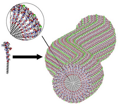
Here, I am describing about how Supramolecular design can help to treat the paralyse problem that occur due to accident. First, we require strong amphiphillic structures which can be designed to form nanocylinders, not tubes or twisted fibrils.Second, it should contain peptide segment that has specific amino acid sequences. Around the fibre, there should be high densities of functional units perpendicular to long axis of fibre, which favours for cell signalling. As these structures are of high concentration, so the main issue will be how to inject this highly viscous substances inside body. We must make them non-viscous outside body, after injecting due to electrolytes presence inside body, it turns into viscous substance inside body which is our requirements. We can change the structures from solution to gel form either by changing pH (making it lower) or by adding electrolytes (due to screening effect of electrolytes, gel formation occurs).

By the recruitment of specific cells from he biological environment into the artificial matrix space and possibly the accumulation at the site of specific proteins, we can trigger regeneration. The nanostructures would be designed to attract specific proteins such as growth factors. A designed nanofiber network is to encapsulate neural progenitor cells and control their differentiation. These progenitor cells have potential to replace the lost CNS cells after degeneration or trauma. Isoleucine-Lysine-Valanine-Alanine-Valine(IKLVAV) are known to promote the neurite sprouting and direct neurite growth. The formation of a bubble gel in which nanofibres surrounds the cells without compromising viability, helps to induce rapid/selective differentiation of progenitor cells into neurons and also suppressed development of astrocytes( cell that impedes the repairing of neurons after spinal cord injury and therefore, block regeneration).

Hence, by this we can stimulate our body for neuron cells regeneration to prevent people from paralysis/disabilities. Upon successful implementation of this kind of regenerative medicine will definitely be a boon in  the field of medical science. Because of the nanotechnology, medical science is progressing a lot and so many complicated issues have been turned to minorities. Still, we have far to go and I hope within 2020, we will be able to change this world into the new era of Nanotechnology.


Tags: , , , , , , ,

MEMS Logic : From translational 3 layer to torsional 2 Layer


During my 2nd semester, I am doing project on designing NEMS logic that has response less than 10 nsec  using COMSOL which later I will characterize NEMS logic at IMEC (Inter-University Microelectronics Centre – Largest Nanotech research Lab in Europe http://www2.imec.be/be_en/home.html ).

NEMS – Nano Electro Mechanical System logic gates are the NEMS devices that can perform Boolean algebra like the logic gates that are composed of solid state transistors (FET, BJT, etc). The proposed NEMS logic gates are expected to have more applications than NEMS switches and also can be used to construct a full-Mechanical computer. The advantages of this mechanical computer over present days computer are that it can work under severe temperatures and strong ion-radiation environments. Under such conditions, conventional solid state transistors that are used in present days computers fails.

The propose of my project is to design a NEMS logic gate that can be fabricated by Surface micro-machining, which uses same mechanical structure to perform either NAND or NOR gate function depending on the electrical interconnects (just by reversing the voltage polarity, NAND gate switch to NOR gate or vice versa). As we know, it is possible to realize entire digital circuitry by NAND and NOR gate functions, so solely from the proposed NEMS logic gate it has potential application to realize mechanical computer.

But, here I am describing about MEMS logic and later I will describe about NEMS logic design after doing researches at IMEC in the upcoming posts.

Translational 3- Layer Design

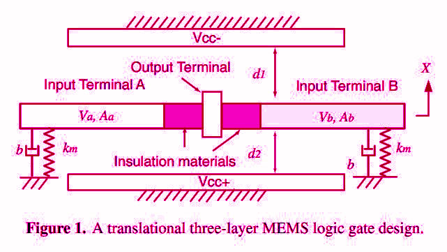
It is shown in figure 1., where the device has one shuttle electrode in the middle and two fixed electrode on the top and bottom. When the fixed electrodes are biased at the voltages of Vcc+ and Vcc-, the shuttle electrode moves either up or down, depending on the voltages applied to it.The output terminal is connected to shuttle electrode which can connect to top or bottom electrode and ultimately gives brings the output. Hence, the logic function in this structure is carried by the motion of shuttle electrode. In this logic gate, there are two gaps d1 and d2 which are different in size, d1>d2 whereas two effective areas Aa and Ab are same. Depending on application of bias at Va and Vb, motion of shuttle occurs and thus following four situations occur.

  1. Va = Vcc+ and Vb= Vcc- : Here voltage difference between upper half and lower half is same but  d1>d2, upper electrostatic force is smaller than down one. The shuttle electrode moves downward and connects the bottom electrode making the output voltage Vcc+.
  2. Va = Vcc- and Vb= Vcc+ : This is the same situation as above so output voltage is Vcc+.
  3. Va = Vcc+ and Vb= Vcc+ : Lower half electrostatic force is zero as there is no voltage drop between bottom electrode and shuttle electrode. So, shuttle electrode moves upward connecting the top electrode making output volatge Vcc-.
  4. Va = Vcc- and Vb= Vcc- : Upper half electrostatic force is zero as there is no voltage drop between top electrode and shuttle electrode. So, shuttle electrode moves downward connecting the bottom electrode making output volatge Vcc+

Hence this gate performs NAND logic (Vcc+ =logic 1 and Vcc- = logic 0) similar to the logic gate composed of solid state transistors. We can switch this NAND logic gate to NOR logic gate by reversing the bias between top and bottom electrode hence can used same mechanical structure for both NAND and NOR logic gate. This structure has no leakage current which is major advantages over FET logic gate. Also output terminal is always connected to either top or bottom electrode so this design has no undefined state which is an issue in some logic devices composed of solid state transistors. However, due to three layered structure, this design is difficult to fabricate by using Surface micromachining. However, this design can be rotated by 90 degree and fabricated by bulk micro machining.


Torsional 2- Layer design

Two layered structure, shown in figure 2, is suitable to fabricate by surface micro-machining which is possible to integrate with existing solid state transistors. Here the shuttle electrode does a see-saw motion which connects the output terminal on each end to export the corresponding output voltage. In three layer design, logic function is controlled by different voltages and different gap whereas in two layer design that is done by different voltages and different dimensions of actuation pad,s Al and Ar.

The actuation torque is always positive for two input signals both at Vcc+ while it is always negative for both input signals at Vcc-. Here micro flexure is designed such that resilient torque remain in between the actuation torque of above both cases. Hence, net torque at (1,1) is always positive and the plate can be actuated from any angle to angle where it connects the output terminal on the right. Similarly, in case (0,0), the plate can be actuated from any angle to angle where it connects the output terminal on the left.

When the input terminals are the combination of either (Vcc+, Vcc-) or (Vcc-, Vcc+) , the plate should be rotated clockwise at any initial angle and then connects the output terminals on the right. Hence, it performs as NOR gate and reversing the voltage polarity at the shuttle electrode it can be switched to NAND gate.

 
Leave a comment

Posted by on February 24, 2011 in MEMS, Nanotech


Tags: , , , , , , , ,

Multigate SOI MOSFETs


The conventional scaling trend for the device, i.e. scaling by reducing device size, is no longer valid for the future generation devices where quantum mechanical effect plays a great role and tunneling and leakage problems will severe the performance of devices. Therefore, scientists are working with different strategies to extend Moore’s Law, such as improving electrostatic control over channel  by means of continued scaling with high K/Metal gate stack and multi gate structures for higher drive current by improving mobility of charge carriers that is done by adopting high mobility channel materials (using Ge or III-V materials) and strain engineering.

Silicon on Insulator transistor has buried oxide layer as soon in figure which plays the main role for providing several advantages. By reducing parasitic drain/source junction capacitances, SOI devices yield improved switching speed and reduced power consumption. By isolating channel from substrate bias effect, it also improves the operating speed. It also provides perfect lateral and vertical isolation from substrate which makes the device free from latch up and inter-device leakage problems.

SOI transistors are of 2 types – PDSOI (partial depleted SOI) and FDSOI ( fully depleted SOI). In PDSOI, silicon film on the BOX layer is thicker than the depletion layer formed beneath the gate oxide, has problems like floating body effects, low threshold voltage variation with temperature as it possess self heating process. This problem has been removed in FDSOI, where silicon film thickness is thin enough or lowly dopes to be fully depleted. However, FDSOI are more sensitive to process variation. One important question is why we are not adopting this properties in present day devices though it has so many several advantages (this ques. was asked by my prof. to me during seminar 😛 ), the reason behind this is the use of FINFET devices which INTEL and TSMC are using in present day devices, which accompanies property like SOI.

In double- gate structure, electric field lines from S/D underneath the device terminate on the bottom of the electrode, and therefore cannot reach the channel region. we can see in the figure that how subthreshold swing has been decreased by the use of double gate structure relative to planar bulk transistor. Double gate structure improves the electrostatic control of gate over channel and no. of equivalent gate is 2 for double gate structure which will provides almost twice drain current than normal planar bulk transistor.
The main advantage of using Multi gate devices is that it supress the drain field much more efficiently. There is a parameter called “Natural length” which  represents length of the region of the channel  that is controlled by drain. Effective gate length should be 5-10 times larger than natural length in order to free from short channel effects. Current drive in Multi Gate FET is equal to current in single gate device times the equivalent no. of gates. So our main purpose is to decrease the natural length parameter. We can see the formula how the natural length parameter depends on dielectric constant of gate oxide and silicon, thickness of silicon and gate oxide. Bu using the no. of equivalent gate, obviously it will decrease the natural length by improving the electrostatic control over channel (i.e. by increasing gate coupling). Also, it proves that how high K material improve the device performance that is obvious by reducing the natural length parameter. In triple gate like pi-Gate and Omega-Gate, equivalent no. of gate is more than 3 (between 3 and 4), hence improve the performance by increasing drain current.
Hence, by using the Multi gate structure in SOI devices, we can improve the performance of transistors by extending Moore’s law and by coupling it with strain engineering, which I discussed in previous section, we can improve mobility of charge carriers much more rapidly, all leads to ultimate high speed of devices.
References:
1. Yong et al, IEEE Vol. 11, No. 3, pp. 93-105, June 25, 2010
2. Colinge et al. Science Direct, Microelectronics engineering 84 (2007) 2071-2076
3. Jurczak et al. IMEC paper, Review of FINFET technology
4. Collaert et al. Solid state electronics 52 (2008) 1291-1296

 
3 Comments

Posted by on February 10, 2011 in CMOS fabrication, Nanotech


Tags: , , , , , , ,

How Intel uses Strain Engineering for Mobility Enhancement


We know that for NMOS transistor, we require tensile strain along channel and  for PMOS, we require compressive strain along channel direction to enhance the mobility of carriers. Due to decrease in dimension of gate length to the few nm scale, short channel effects causes severe degradation in the performance of transistors. Carriers velocity saturates soon which limit the drain current and slow down the devices. Intel got a dramatic performance enhancement in strained channel relative to unstrained one. Intel uses this strain engineering techniques to the transistors having gate length of 45 nm and 50 nm for NMOS and PMOS respectively, accompanied with 1.2 nm gate oxide and Ni salicide. I already mentioned in previous artice that salicide are used to lower the parasitic resistance but here it helps on providing tensile strain along NMOS channel also to enhance the mobility of electrons.

In PMOS, Intel embeds compressively strained SiGe film in the source drain regions by using the selective epitaxial growth process. A combination of compressive SiGe strain and embedded SiGe S/D geometry induces a large uniaxial compressive strain in the channel region, thereby resulting in significant hole mobility improvement. We can see from the figure that on deposition of SiGe film, it produces force laterally which provide stress such that channel length reduces in size providing compressive nature of strain. Such strain causes the change in band structure such that curvature of band increases causing lower in the effective mass of hole and as mobility is inversely proportional to effective mass which ultimately enhance the mobility of hole.

For NMOS, Intel integrate a post salicide “highly-tensile” silicon nitride capping layer due to which the stress from this capping layer is uniaxially transferred to the NMOS channel through the source-drainregions to create tensile strain in NMOS channel. Due to deposition of SiN capping layer, it provide stress to channel region such that it elongates the channel region so called tensile strain which will ultimately change the band structure such that it increases the mobility of electron and hence the performance of NMOS devices.

Hence, the combined techniques of selective SiGe source-drainand high stress silicon nitride capping layer are low cost and highly manufacturable means to induce strain in transistors and allow for separate optimization of PMOS and NMOS devices. Only troublesome to this strain engineering is that we require selective growth process separately for NMOS and PMOS which are core components of CMOS and to integrate them within same substrate is really costly.

References:

[1]. Ghani et al. Intel paper
[2]. K. Rim et al., Symp. VLSI Tech Dig.., pp. 98-99, (2002)
[3]. S. Thompson et al., IEDM Tech Dig., pp. 61-64, (2002)
[4]. S. Ito et al., IEDM Tech Dig., pp. 247-251, (2000)
[5]. A. Shimizu et al., IEDM Tech Dig., pp. 433-437, (2001)

 
3 Comments

Posted by on February 10, 2011 in CMOS fabrication


Tags: , , , , , , , , , , ,

Challenges and solutions to present CMOS complexities


Every people have noticed increase in speed of present technologies, decrease in their price and more slimmer and slimmer devices they are able to use. However, rarely people know about the challenges and complexities scientists are facing just to model a transistor in few nm range and then to fabricate them in chips ultimately by integrating billions of transistors. I have seen how scientists are working on it by sacrificing their entertaining life and totally plunge their life in researches.

Presently we are using Intel chip of 45 nm, this length actually corresponds to dimensions of gate length transistor. More we decrease the size of transistor, classical law fails to follow and ultimately quantum mechanical phenomenon comes into picture. Gate tunneling leakage, Interdevice leakage, scattering phenomenon – all leads to dissipation of power and ultimately accumulation of heat from billions of transistors which ultimately can burn your PC/laptops. Intel, TSMC, these famous companies they are able to fabricate 22 nm transistors and even smaller but the main problem is how to take control over heat accumulation. We can have high performance devices but care must be taken over to reduce power consumption and to control heat production.

These are major problems which we are facing with present planar bulk MOSFET given below.

1.Poor Electrostatics ⇒ Increased Ioff, leakage current from reverse biased diode formed at drain to substrate junction can reach to channel and ultimately make poor electrostatics control over channel.
–Solution: Double Gate, which increases electrostatic control over channel and increase the drain current. Leakage current terminate over lower gate and can’t go to channel region.
2.Poor Channel Transport ⇒ decreased Ion, More we reduce the length of channel, scattering will increase that will saturate the velocity of electrons earlier than saturation drain current.
–Solution – High Mobility Channel /Strain engineering, we can use high mobility channel like Ge on Si epitaxy as we know for Ge, electron mobilty is very high because of its lower effective mass even lower than that of hole. By tensile strain along NMOS channel or compressive strain along PMOS channel, we can increase mobility of charge carriers and ultimately it will increase ON current and hence increase the performance.
3. S/D Parasitic resistance ⇒ decreased Ion current
–Solution – Metal Silicides, as we know silicides have very low resistance and it also improve mobility of charge carriers by providing strain over channel.
4. Gate leakage increased, as thickness of SiO2 goes below 2 nm, tunneling effect comes into picture which causes large leakage current. To increase the speed of transistor, we need to increase Ion for that we need to increase Gate coupling capacitance for which ultimately we need to decrease the thickness of gate oxide.
–Solution – High-K dielectrics –  Because of high dielectric, it increases the gate coupling capacitance and we can have thicker gate dielectric between gate and channel that will ultimately improve the performance of device. Nitrided Hafnium silicon oxide have found to be best alternative for high K dielectic.
5.Gate depletion ⇒ increased EOT, because of depletion layer formed between Poly and gate dielectric, additional capacitance is formed in series which ultimately increase the Equivalent oxide thickness(EOT), which is equivalent thickness of gate oxide of gate dielectric that can produce same current, and hence reduce the performance.
–Solution – Metal gate, it prevents the formation of depletion layer so High K- Metal stack is found to be best alternative for poly-gate oxide stack.
Other interesting solutions are Multigate Silicon on Insulator transistor, FINFET, CNT based FET and soon which can overcome present days problems which I will discuss in next chapter in details.
 
2 Comments

Posted by on February 7, 2011 in CMOS fabrication


Tags: , , , , , , , , , , , , ,

Superconductivity theory


Superconductivity is a phenomenon in which material possess zero resistance below critical temperature, which is mostly very low temperature.

Electrical current in a superconducting ring can persist for an infinitely long time. Let at T>Tc, ring is placed in an external magnetic field so that field lines passes through the interior  of ring, Ring is cooled down below critical temperature, Tc, and external  magnetic field is switched off. At first moment, magnetic flux through the ring decreases but according to the Faraday laws of electromagnetic induction, it induces current in a ring which will be persistent throughout which actually prevents decrease in magnetic flux through the ring. If the ring has resistance, flux would decay with time (L/R). In superconducting ring, R=0 so current will take infinite time to decay that means current will be persistent throughout. This is the case of frozen Magnetic flux.

Meissner-Ochsenfeld effect

Weak enough magnetic field is applied to ideal conductor(Super conductor) so that field will not destroy the super conductor and it is cooled down below Tc in zero magnetic field. After external magnetic field is applied, field doesn’t penetrate the interior of sample. As soon as field starts penetrating, instantly an induced current is set up by Lenz’s law which generates the magnetic field in the direction opposite to external field. Hence, total field inside the interior of sample is zero. This is called Meissner-Ochsefeld effect.

If we apply magnetic field greater than critical value, then it will destroy superconductivity.

Transition to Superconductor is a phase transition at which superconductor shows diamagnetism. There are two type of Superconductor – Type I (mostly all metals except Noibium) and Type II (Noibium and superconducting alloys)

Type II superconductors do not show Meissner-Ochsenfeld effect. When magnetic field is increased from zero, at first it pushes out all the field and shows Meissner effect until Ho<Hc1, lower critical field. Further increase of magnetic field Ho, induction B build up and becomes equal B=Ho at H=Hc2, upper critical field. However in a thin surface layer, the superconductivity will remain even at Ho>Hc2 until H0=1.69Hc2. This field is strong enough to destroy superconductivity in the surface layer as well. It is called 3rd critical field Hc3.

Superconducting state is more ordered state than normal one because it is characterised by lower entropy. Transition at T=Tc doesn’t involve latent heat because entropy at superconductor and normal state are equal in the absence of magnetic field so that it is called 2nd order phase transition.

However, at T<Tc, a transition from superconducting state to normal state occurs, when a sufficiently strong magnetic field is applied. At this case, entropy of superconducting state is much lower than that of normal one, such transition is accompanied by absorption of latent heat. Therefore, in presence of magnetic field, all the transition at T<Tc are 1st order transitions.

Superconductivity is based on cohorent behaviour of electrons. Two basic properties of superconductivity are absolute diamagnetism and zero resistance to DC current. According to London theory, electrons in Superconductor may be considered as mixture of two groups; superconductor electrons and normal electrons. Number density of superconductor electrons, Ns decreases with increasing temperature and eventually becomes zero at T=Tc. In presence of AC electric field, both normal and superconductor components of currents are finite and the normal current obeys ohm’s law. Therefore, real superconductor can be modeled as series connection  of normal resistor and ideal conductor.

Ginzburg Landaeu Theory

It introduced quantum mechanics into the description of superconductors. Entire superconducting electrons are described as a function of n coordinates Ψ(r1,r2,r3,…). It establishes cohorent behaviour of all superconducting electrons. GL theory was built on the basis of theory of 2nd order phase transitions which is valid only at the vicinity of Tc in the range Tc-T<<Tc. Having applied GL theory to superconducting alloys, Abrikosov developed a theory of so called Type II superconductor. Superconductors do not necessarily have surface energy > zero. Those do have surface energy > zero are Type I superconductors. Majority of Superconducting alloys and chemical compounds show surface energy < zero ehich are called Type II superconductors.

For Type II superconductors, magnetic field penetrate inside the material in the form of quantised vortex lines which is the quantum effect on macroscopic scale). Superconductivity in these materials can survive upto high magnetic fields.

BCS Theory

This theory takes into account the interaction between electrons and phononsn also demonstrate electron-electron attraction which is due to exchange of phonons and formed Cooper Pairs whose total spin is zero that represent Boson particle, hence obeys Bose-Einstein statistics. For such particle, if the temperature fall below Tc, they can all gather at lowest energy level, Ground state. Larger the no. of particles that have accumulated there, more difficult it is for one of them to leave this state. This process is called Bose-Einstein Condensation. All the particles in the condensate have same wave function. Flows of condensate must be superfluid that is dissipation free. Not easy for one to be scattered, 1st have to overcome resistance of the rest of the condensate. Thus at T<Tc, there exist a condensate of Cooper pairs which is superfluid, i.e. dissipation free electric current is carried by Cooper pairs. Charge of elementary carrier is 2e.

Cohorence length and Penetration depth

Let the film of a normal metal is deposited onto a clean flat surface of the superconductor. It cause reduction in the superconducting electron density near the surface of superconductor. In other words, Order parameter. |Ψ| at the surface will somewhat different from its equilibrium value deep inside the superconductor, whee |Ψ|=1.

Cohorence length is the characteristics length over which order parameter returns to unity or over which variations of order parameter |Ψ| occurs. Penetration depth is the distance upto which magnetic field penetrates.

Weak Superconductivity

Weak superconductivity refers to the situation in which two superconductor are coupled together by a weak link that provide a tunnel junction, provided that width if weak link is less than cohorence length which causes that order parameter from one superconductor can feel that of other one. This phenomenon is called Josephson effect. There are two types of Josephson effect:

a) DC Josephson effect : There is a certain phase difference across the weak link which causes the production of +ve and -ve current, Ic.

b) AC Josephson effect: When voltage is applied across the junction, then phase starts varying with time which also causes current to vary over time so produce oscillation in current which is called ac current.

Application of Weak superconductivity – DC squid, which is used to measure very small magnetic field.


1 Comment

Posted by on February 5, 2011 in Superconductivity


Tags: , , , , , , , , , , , , , , , , , , , , , , ,

Encoded nanopore for single molecule detection and Enantiomers discrimination


Presently, I am doing research on encoded nanopore which can be used as nano sensor for single molecule detection and can also be used to discriminate the enantiomers. Abstract is as follows:

Nanopore, pore with dimension of nm, serves as ultra sensitive novel devices for sensing the single molecule. The principle driving this nano sensor is that when a target molecule traverses or binds in the lumen nanopore, they characteristically block the ion pathway, resulting change in conductance of target specific. The characteristics change in conductance is unique for each type of molecules, therefore serving as a fingerprint for target identification and quantification. This nanopore technology can provide unique biosensing platforms for detecting nucleic acid (DNA)  and peptide molecules, high precision of molecular transportation like in drug delivery and the study of single molecule chemistry.

Protein pores that have receptors attached to them are target-selective, but their real-time applications are limited by the fixed pore size and fragility of the lipid membrane into which the protein pores are embedded. Also, synthetic nanopores are more stable and provide flexible pore sizes, but the selectivity is low when detecting in the translocation mode. Even though the nanopore has been functionalized with recognizing groups such as antibodies, these nanopores fail to bind individual target molecules. Distinguishing between binding and translocation blocks remains unsolved.

Aptamers, or “synthesized antibodies,” which are short DNA or RNA segments that are created by in vitro evolution and have high sensitivity and selectivity, are encoded in the nanopore which has several advantages like:more durable than most protein receptors, simpler to synthesize, modify, and immobilize using low cost methods. In contrast to antibodies, aptamers are much smaller than their targets, rendering target blockades in the nanopore much more distinguishable.

Selectivity can be checked by comparing   the response of AIgE/A-ricin-modified nanopore in different molecular species, where block like characteristics that are seen in original form can’t be obtained. This nanopore adopts the receptor attachment mode, rather than the molecular translocation mode, for single-molecule detection. Only molecules that are recognized by the immobilized receptor are able to yield featured block signals, providing high selectivity. The pore size does not need to match the target molecule dimension. Also it has increased the detection sensitivity to ~100 fM. We can also discriminate the enantiomers as R and S enantiomers have different current characteristics like one having more reduced current than others with narrower amount of time.

For future applications, these can be particularly useful in real-time applications- the digital signal of the discrete blocks distinguishes them from the analog background signal, hence possibility of real time sensor.


References:

1. Gu et al.,” Aptamer encoded nanopore for Ultrasensitive Detection of Bioterrorist Agent Ricin at Single Molecule Detection” , IEEE EMBS Journal, 2009,  6699-6702
2. Ding et al.,”Capturing single molecule of Immunoglobulin and Ricin with an Aptamer encoded Glass Nanopore”, Anal Chem, 2009, 81, 6649-6655
3. Gao et al. “A simple method of creating a nanopore-terminated probe for single-molecule enantiomer discrimination”, Anal Chem., 2009, 81, 80-86
 
Leave a comment

Posted by on November 25, 2010 in Bio-nanotech


Tags: , , , , , , , , , , , , , , , , ,

Quantum entanglement and teleportation


Dec 29th 1959, Physicist Richard Feynman gave wonderful lecture entitled “There is plenty of room at the bottom” at an American Physical Society meeting at Caltech, where he presented a audacious and enduring vision of a technological advancements leading toward the atomic scale and toward the ultimate boundaries set by laws of physics. The world has traveled far toward what Feynman saw, and has far still to go. The way things are in the atomic world  is totally different to large scale objects like bike and engines. We can’t rely on experience and common sense to guide us on how things are going to work at this level. And that can make some of the effects of quantum physics seem mystical and one of the strangest features is quantum entanglement.

Quantum entanglement, a bizarre feature of quantum physics, is a phenomenon where there is possibility of linking two quantum particles  like photons, gravitons or atoms in a special way such that they act effectively two parts of the same entity. We can then separate them to the extent that we like and change in one is instantly reflected in the other. The link of entanglement works instantaneously at any distance. So it would be spooky action if it could be used to send a signal.  Entanglement can be measured, transformed, and purified. A pair of quantum systems in an entangled state can be used as a quantum information channel to perform computational and cryptographic tasks.

According to quantum mechanics, we can have range of possibilities each having certain probabilities and state remain undefined until it is measured. Only after observation, we can acquire defined state and state of other possibilities is destroyed. Entanglement link is also based on probabilities. For spin entangled atoms, we can’t realize the state of atom accurately until it is measured as they have range of probabilities on the values of their properties. Suppose x and y are entangled pair and they are separated to the extent we wish. If one of the atom x is measured spin up then without measuring we can predict that another atom y is at spin down state instantly. After measurement, wave function, that describes the complex probability amplitudes of the two particles together, of those entangled pair is collapsed, no matter how far they are. We can generate such pair of entangled spin +1 and -1 by making collision of pair of spin 0 atoms and these will increase their kinetic energy to compensate for their loss of spin energy. After each of these collisions, the two fast moving entangled atoms will then head straight out of the atom trap in opposite directions.

Scientists in China have already succeeded in teleporting information between photons over free space distance of 10 miles, much further than the few hundred metres previously achieved. In most of the experiments related to teleportation, photon has been used. Here, two photons are used which are entangled in such way that if one’s quantum state is changed, the state of other also changes instantaneously. In latest experiments in China, pair of photons were entangled in the spatial modes of photon 1 & polarization modes of photon 2 and two types of telescopes were designed in which one serves as optical transmitting antenna and other as optical receiving antenna.

It has been predicted that minimum speed for entanglement is 10000 times the speed of light. However, according to Einstein’s theory of relativity, anything traveling faster than light would be going back in time. Einstein said there is an inverse proportion between speed and light, and that if one were to reach the speed of light time would stop. Therefore if you exceed the speed of light you would be travelling back in time. Of course there is always the possibility  that Einstein was wrong about that. If he is true then information can be sent back to the past. But what will be consequences? If that is possible there must be cause and effect and consequences are horrible. That’s why quantum physics is full of absurdness.

Although these entangled pairs are able to communicate successfully, we can’t state precisely what actually has been transmitted.  It has always been challenging tasks to develop a precise detector. To receive the information and to interpret it are different processes. Chinese talks are not exact information for us until we can interpret. It means though information was transferred, if we can’t interpret it then that is no more information for us.

There’s a fundamental problem associated with quantum teleportation. Because looking at a quantum particle changes it. We can’t scan a particle, see what it looks like and make an exact copy. So it might seem that teleportation is impossible. Entanglement let us get around this restriction.We can interact the particle with one half of an entangled pair, and then putting the other half of the pair through a special process, a bit like a logic gate in a computer, it’s possible to make an identical particle at a remote location. We can only do this because the entanglement transfers the quantum information without us ever knowing what it was. In the process, the original particle loses its properties.  That’s means it follow cut and paste rule rather than copy and paste.

Does it possible to teleport human body in future?

Quantum entanglement is an experimentally verified fact. Human body comprises of billions and billions of such quantum particles. There has got to be a bunch of entangled particles somewhere in the universe. Luck, intution, telepathy, sympathy, empathy, love, hate, ego are a result of quantum teleportation into our minds.  What we see in our dreams is also an effect of quantum teleportation from a distant particle. So if quantum teleportation can be precisely realised in future, it is possible to think about the concept of time machine. Human beings will not only able to be teleported but also able to travel in time machine. But it seems totally filled with absurdness.

References:

  1. Zeilinger, A.; IEEE paper, “Quantum entanglement and information Quantum Electronics and Laser Science Conference, 2000. (QELS 2000). Technical Digest Publication Year: 2000
  2. Weinfurter, H.; Bouwmeester, D.; Daniell, M.; Jennewein, T.; Jian-Wei Pan; Simon, C.; Weihs, G.; Zeilinger, A.; “Quantum communication and entanglement“ Circuits and Systems, 2000. Proceedings. ISCAS 2000 Geneva. The 2000 IEEE International Symposium on Volume: 2 Digital Object, Publication Year: 2000 , Page(s): 236 – 239 vol.2
  3. Prakash, H.; IEEE paper, “ Quantum Teleportation”Emerging Trends in Electronic and Photonic Devices & Systems, 2009. ELECTRO ’09. International Conference on Publication Year: 2009 , Page(s): 18 – 23
  4. http://www.physorg.com/news193551675.html
  5. http://quantumartandpoetry.blogspot.com/2009/04/paradoxes-of-quantum-mechanics.html
  6. http://www.daviddarling.info/encyclopedia/Q/quantum_entanglement.html
 
4 Comments

Posted by on July 27, 2010 in Nanotech, Quantum Mechanics


Tags: , , , , , , , ,